


参数搜索
Medium-voltage GaN (80 - 200 V)
 数据加载中,请稍候...
参数搜索不可用。
产品
| 型号 | 描述 | 状态 | 快速访问 |
|---|---|---|---|
| GAN3R2-100CBE | 100 V, 3.2 mOhm Gallium Nitride (GaN) FET in a 3.5 mm x 2.13 mm Wafer Level Chip-Scale Package (WLCSP) | Production | |
| GAN7R0-150LBE | 150 V, 7 mOhm Gallium Nitride (GaN) FET in a 2.2 mm x 3.2 mm x 0.774 mm Land Grid Array (LGA) package | Production | |
| GANE011-080CBA | AEC-Q101 qualified 80 V, 11 mOhm Gallium Nitride (GaN) FET in a 1.5 mm x 1.5 mm Wafer Level Chip-Scale Package (WLCSP) | Production | |
| GANE0R8-100QTM | 100 V, 0.75 mOhm Gallium Nitride (GaN) FET in a QFN 3 mm x 5 mm TSC package | Development | |
| GANE1R2-100QTM | 100 V, 1.2 mOhm Gallium Nitride (GaN) FET in a QFN 3.3 mm x 3.3 mm TSC package | Development | |
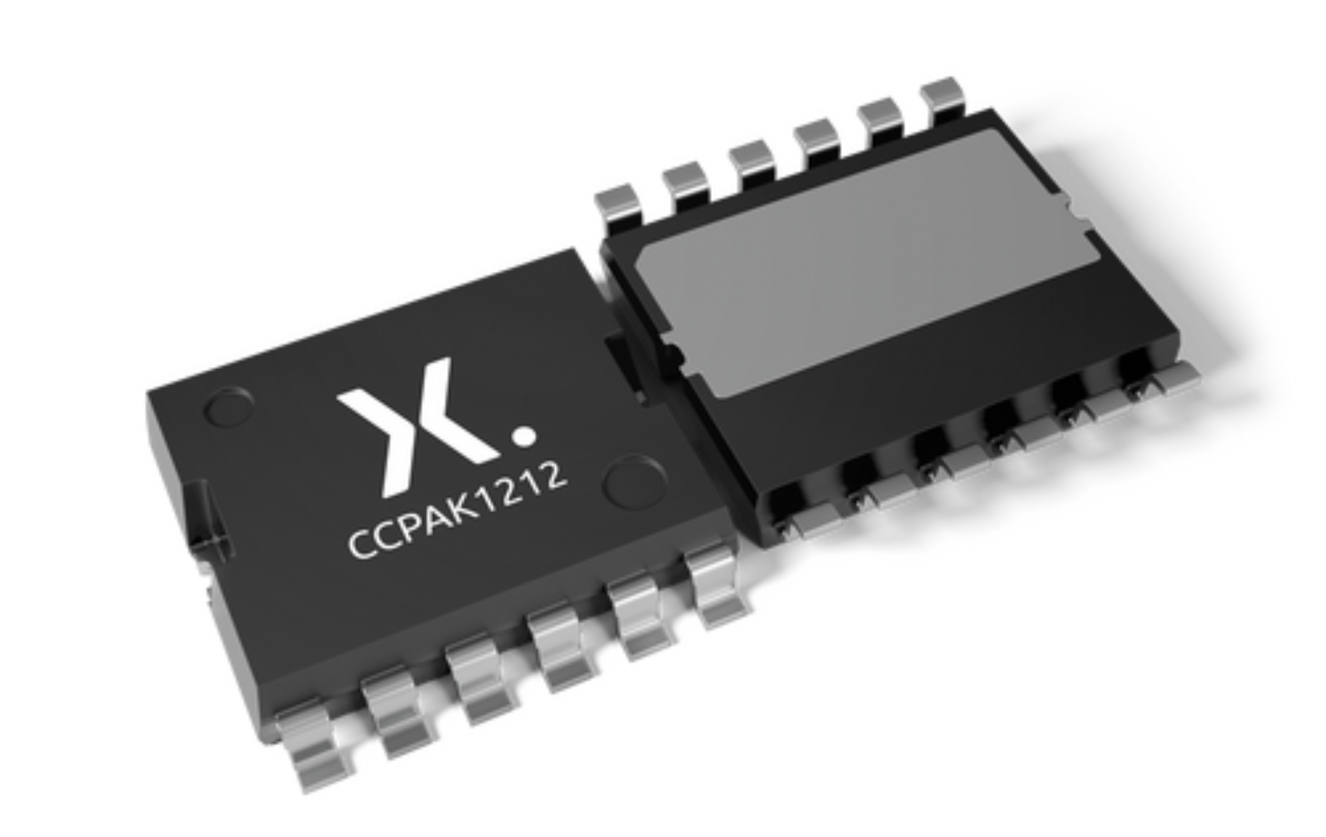
| GANE1R8-100QBA | 100 V, 1.8 mOhm Gallium Nitride (GaN) FET in a 4.0 mm x 6.0 mm Very-Thin-Profile Quad Flat No-Lead Package (VQFN) | Production | |
| GANE2R7-100CBA | 100 V, 2.7 mOhm Gallium Nitride (GaN) FET in a 4.45 mm x 2.30 mm Wafer Level Chip-Scale Package (WLCSP) | Production | |
| GANE3R5-200QTM | 200 V, 3.5 mOhm Gallium Nitride (GaN) FET in a QFN 3 mm x 5 mm TSC package | Development | |
| GANE3R9-150QBA | 150 V, 3.9 mOhm Gallium Nitride (GaN) FET in a 4.0 mm x 6.0 mm Very-Thin-Profile Quad Flat No-Lead Package (VQFN) | Production | |
| GANE7R0-100CBA | 100 V, 7.0 mOhm Gallium Nitride (GaN) FET in a 2.5 mm x 1.5 mm Wafer Level Chip-Scale Package (WLCSP) | Production | |
| GANE7R2-200QTM | 200 V, 7.2 mOhm Gallium Nitride (GaN) FET in a QFN 3 mm x 5 mm TSC package | Development |
Visit our documentation center for all documentation
Application note (1) |
|||
|---|---|---|---|
| 文件名称 | 标题 | 类型 | 日期 |
| AN90021.pdf | Power GaN technology: the need for efficient power conversion | Application note | 2020-08-14 |
Leaflet (1) |
|||
| 文件名称 | 标题 | 类型 | 日期 |
| nexperia_document_leaflet_GaNFETs_2026.pdf | Power GaN FETs | Leaflet | 2026-10-01 |
Marcom graphics (1) |
|||
| 文件名称 | 标题 | 类型 | 日期 |
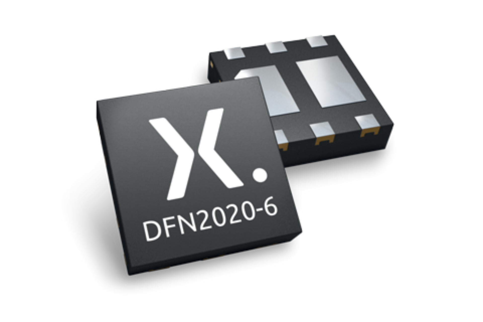
| WLCSP8_SOT8072-combi_mk.png | wafer level chip-scale package; 8 solder bars; body: 3.5 x 2.13 x 0.429 mm | Marcom graphics | 2023-04-20 |
White paper (4) |
|||
| 文件名称 | 标题 | 类型 | 日期 |
| nexperia_document_whitepaper_48V_motor_drives_with_GaN_2026.pdf | Whitepaper: Enabling high-efficiency 48 V motor drives with GaN: Diode-less operation and ultra-short dead time in 70 A / 100 kHz systems | White paper | 2026-10-07 |
| nexperia_whitepaper_gan_need_for_efficient_conversion_Japanese.pdf | Whitepaper: GaN need for efficient conversion (Japanese) | White paper | 2021-05-20 |
| nexperia_whitepaper_gan_need_for_efficient_conversion_CHN.pdf | 白皮书: 功率GaN技术: 高效功率转换的需求 | White paper | 2020-08-17 |
| nexperia_whitepaper_gan_need_for_efficient_conversion.pdf | White paper: Power GaN technology: the need for efficient power conversion | White paper | 2020-07-23 |