
参数类型
| 型号 | VCC (V) | Logic switching levels | Output drive capability (mA) | tpd (ns) | fmax (MHz) | Nr of bits | Power dissipation considerations | Tamb (°C) | Rth(j-a) (K/W) | Ψth(j-top) (K/W) | Rth(j-c) (K/W) | Package name |
|---|---|---|---|---|---|---|---|---|---|---|---|---|
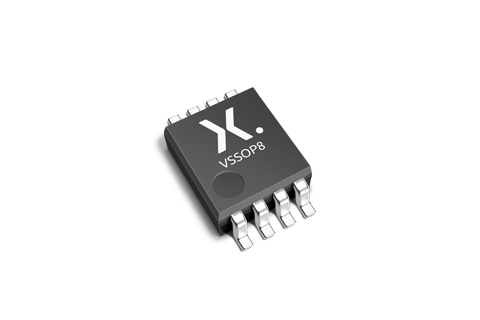
| 74AUP1G885DC | 0.8 - 3.6 | CMOS | ± 1.9 | 7.6 | 70 | 1 | ultra low | -40~125 | 203 | 34.1 | 113 | VSSOP8 |
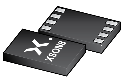
| 74AUP1G885GN | 0.8 - 3.6 | CMOS | ± 1.9 | 7.6 | 70 | 1 | ultra low | -40~125 | 238 | 10.6 | 148 | XSON8 |
| 74AUP1G885GS | 0.8 - 3.6 | CMOS | ± 1.9 | 7.6 | 70 | 1 | ultra low | -40~125 | 276 | 10.8 | 146 | XSON8 |
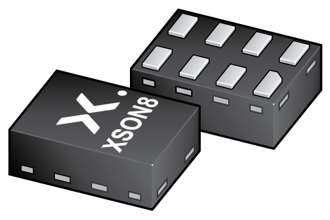
| 74AUP1G885GT | 0.8 - 3.6 | CMOS | ± 1.9 | 7.6 | 70 | 1 | ultra low | -40~125 | 327 | 6.1 | 157 | XSON8 |
封装
| 型号 | 可订购的器件编号,(订购码(12NC)) | 状态 | 标示 | 封装 | 外形图 | 回流焊/波峰焊 | 包装 |
|---|---|---|---|---|---|---|---|
| 74AUP1G885DC | 74AUP1G885DC,125 (935280765125) |
Active | pS8 |
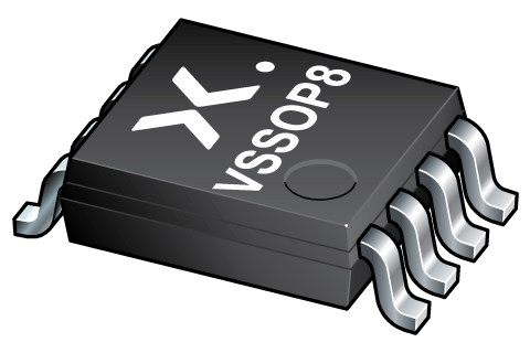
VSSOP8 (SOT765-1) |
SOT765-1 | SOT765-1_125 | |
| 74AUP1G885GN | 74AUP1G885GN,115 (935292216115) |
Active | 58 |
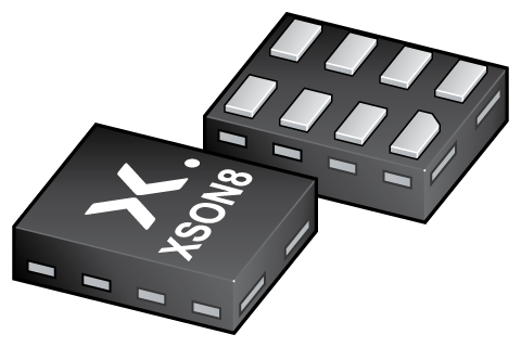
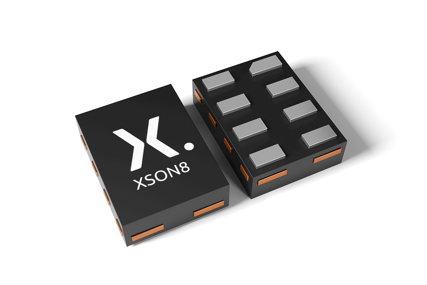
XSON8 (SOT1116) |
SOT1116 |
REFLOW_BG-BD-1
|
SOT1116_115 |
| 74AUP1G885GS | 74AUP1G885GS,115 (935292777115) |
Active | 58 |
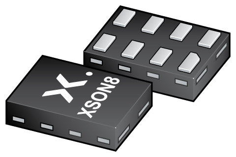
XSON8 (SOT1203) |
SOT1203 |
REFLOW_BG-BD-1
|
SOT1203_115 |
| 74AUP1G885GT | 74AUP1G885GT,115 (935280767115) |
Active | pS8 |
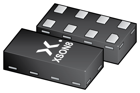
XSON8 (SOT833-1) |
SOT833-1 | SOT833-1_115 |
下表中的所有产品型号均已停产 。
| 型号 | 可订购的器件编号,(订购码(12NC)) | 状态 | 标示 | 封装 | 外形图 | 回流焊/波峰焊 | 包装 |
|---|---|---|---|---|---|---|---|
| 74AUP1G885GD | 74AUP1G885GD,125 (935288876125) |
Obsolete | pS8 Standard Procedure Standard Procedure |
XSON8 (SOT996-2) |
SOT996-2 | SOT996-2_125 | |
| 74AUP1G885GF | 74AUP1G885GF,115 (935291472115) |
Withdrawn / End-of-life |
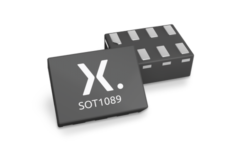
XSON8 (SOT1089) |
SOT1089 |
REFLOW_BG-BD-1
|
SOT1089_115 | |
| 74AUP1G885GM | 74AUP1G885GM,125 (935280766125) |
Obsolete | pS8 |
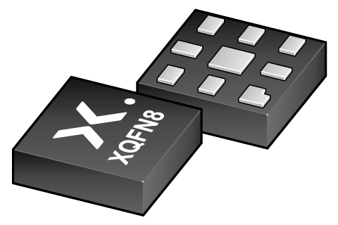
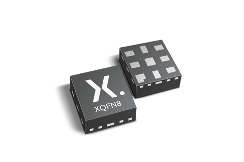
XQFN8 (SOT902-2) |
SOT902-2 | SOT902-2_125 |
环境信息
| 型号 | 可订购的器件编号 | 化学成分 | RoHS | RHF指示符 |
|---|---|---|---|---|
| 74AUP1G885DC | 74AUP1G885DC,125 | 74AUP1G885DC |
|
|
| 74AUP1G885GN | 74AUP1G885GN,115 | 74AUP1G885GN |
|
|
| 74AUP1G885GS | 74AUP1G885GS,115 | 74AUP1G885GS |
|
|
| 74AUP1G885GT | 74AUP1G885GT,115 | 74AUP1G885GT |
|
|
下表中的所有产品型号均已停产 。
| 型号 | 可订购的器件编号 | 化学成分 | RoHS | RHF指示符 |
|---|---|---|---|---|
| 74AUP1G885GD | 74AUP1G885GD,125 | 74AUP1G885GD |
|
|
| 74AUP1G885GF | 74AUP1G885GF,115 | 74AUP1G885GF |
|
|
| 74AUP1G885GM | 74AUP1G885GM,125 | 74AUP1G885GM |
|
|
文档 (33)
| 文件名称 | 标题 | 类型 | 日期 |
|---|---|---|---|
| 74AUP1G885 | Low-power dual function gate | Data sheet | 2024-08-12 |
| AN10161 | PicoGate Logic footprints | Application note | 2002-10-29 |
| AN11052 | Pin FMEA for AUP family | Application note | 2019-01-09 |
| AN90063 | Questions about package outline drawings | Application note | 2025-03-12 |
| 001aah898 | Block diagram: 74AUP1G885DC, 74AUP1G885GD, 74AUP1G885GM, 74AUP1G885GT | Block diagram | 2009-11-04 |
| Nexperia_document_guide_MiniLogic_PicoGate_201901 | PicoGate leaded logic portfolio guide | Brochure | 2019-01-07 |
| Nexperia_document_guide_MiniLogic_MicroPak_201808 | MicroPak leadless logic portfolio guide | Brochure | 2018-09-03 |
| SOT765-1 | 3D model for products with SOT765-1 package | Design support | 2020-01-22 |
| SOT1089 | 3D model for products with SOT1089 package | Design support | 2019-10-07 |
| SOT1116 | 3D model for products with SOT1116 package | Design support | 2023-02-02 |
| SOT1203 | 3D model for products with SOT1203 package | Design support | 2023-02-02 |
| SOT833-1 | 3D model for products with SOT833-1 package | Design support | 2021-01-28 |
| aup1g885 | aup1g885 IBIS model | IBIS model | 2013-04-07 |
| Nexperia_document_Logic_CombinationLogic_infocard_201710 | Combination logic solutions card | Leaflet | 2019-08-09 |
| Nexperia_document_leaflet_Logic_AUP_technology_portfolio_201904 | Nexperia_document_leaflet_Logic_AUP_technology_portfolio_201904 | Leaflet | 2019-04-12 |
| Nexperia_package_poster | Nexperia package poster | Leaflet | 2020-05-15 |
| VSSOP8_SOT765-1_mk | plastic, very thin shrink small outline package; 8 leads; 0.5 mm pitch; 2 mm x 2.3 mm x 1 mm body | Marcom graphics | 2017-01-28 |
| XSON8_SOT1089_mk | plastic, extremely thin small outline package; no leads; 8 terminals; 0.55 mm pitch; 1.35 mm x 1 mm x 0.5 mm body | Marcom graphics | 2017-01-28 |
| XQFN8_SOT902-2_mk | plastic, extremely thin quad flat package; 8 terminals; 0.55 mm pitch; 1.6 mm x 1.6 mm x 0.5 mm body | Marcom graphics | 2017-01-28 |
| XSON8_SOT1203_mk | plastic, leadless extremely thin small outline package; 8 terminals; 0.35 mm pitch; 1.35 mm x 1 mm x 0.35 mm body | Marcom graphics | 2019-02-04 |
| SOT765-1 | plastic, very thin shrink small outline package; 8 leads; 0.5 mm pitch; 2 mm x 2.3 mm x 1 mm body | Package information | 2022-06-03 |
| SOT996-2 | plastic, leadless extremely thin small outline package; 8 terminals; 0.5 mm pitch; 3 mm x 2 mm x 0.5 mm body | Package information | 2020-04-21 |
| SOT1089 | plastic, leadless extremely thin small outline package; 8 terminals; 0.35 mm pitch; 1.35 mm x 1 mm x 0.5 mm body | Package information | 2022-06-03 |
| SOT902-2 | plastic, leadless extremely thin quad flat package; 8 terminals; 0.5 mm pitch; 1.6 mm x 1.6 mm x 0.5 mm body | Package information | 2020-04-21 |
| SOT1116 | plastic, leadless extremely thin small outline package; 8 terminals; 0.3 mm pitch; 1.2 mm x 1 mm x 0.35 mm body | Package information | 2022-06-02 |
| SOT1203 | plastic, leadless extremely thin small outline package; 8 terminals; 0.35 mm pitch; 1.35 mm x 1 mm x 0.35 mm body | Package information | 2022-06-03 |
| SOT833-1 | plastic, leadless extremely thin small outline package; 8 terminals; 0.5 mm pitch; 1 mm x 1.95 mm x 0.5 mm body | Package information | 2022-06-03 |
| REFLOW_BG-BD-1 | Reflow soldering profile | Reflow soldering | 2021-04-06 |
| Nexperia_Selection_guide_2023 | Nexperia Selection Guide 2023 | Selection guide | 2023-05-10 |
| MAR_SOT1089 | MAR_SOT1089 Topmark | Top marking | 2013-06-03 |
| MAR_SOT1116 | MAR_SOT1116 Topmark | Top marking | 2013-06-03 |
| MAR_SOT1203 | MAR_SOT1203 Topmark | Top marking | 2013-06-03 |
| MAR_SOT833 | MAR_SOT833 Topmark | Top marking | 2013-06-03 |
支持
如果您需要设计/技术支持,请告知我们并填写 应答表 我们会尽快回复您。
模型
| 文件名称 | 标题 | 类型 | 日期 |
|---|---|---|---|
| SOT765-1 | 3D model for products with SOT765-1 package | Design support | 2020-01-22 |
| SOT1089 | 3D model for products with SOT1089 package | Design support | 2019-10-07 |
| SOT1116 | 3D model for products with SOT1116 package | Design support | 2023-02-02 |
| SOT1203 | 3D model for products with SOT1203 package | Design support | 2023-02-02 |
| SOT833-1 | 3D model for products with SOT833-1 package | Design support | 2021-01-28 |
| aup1g885 | aup1g885 IBIS model | IBIS model | 2013-04-07 |
Ordering, pricing & availability
样品
作为 Nexperia 的客户,您可以通过我们的销售机构订购样品。
如果您没有 Nexperia 的直接账户,我们的全球和地区分销商网络可为您提供 Nexperia 样品支持。查看官方经销商列表。