
参数类型
| 型号 | VCC (V) | Logic switching levels | Output drive capability (mA) | tpd (ns) | fmax (MHz) | Nr of bits | Power dissipation considerations | Tamb (°C) | Rth(j-a) (K/W) | Ψth(j-top) (K/W) | Package name |
|---|---|---|---|---|---|---|---|---|---|---|---|
| 74AUP2G97DP | 0.8 - 3.6 | CMOS | ± 1.9 | 8.7 | 70 | 2 | ultra low | -40~125 | 120 | 30 | TSSOP10 |
| 74AUP2G97GU | 0.8 - 3.6 | CMOS | ± 1.9 | 8.7 | 70 | 2 | ultra low | -40~125 | 142 | 48 | XQFN10 |
封装
| 型号 | 可订购的器件编号,(订购码(12NC)) | 状态 | 标示 | 封装 | 外形图 | 回流焊/波峰焊 | 包装 |
|---|---|---|---|---|---|---|---|
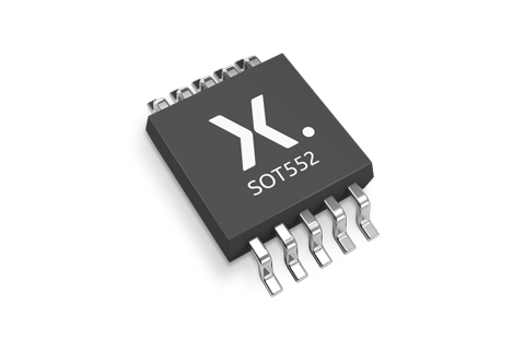
| 74AUP2G97DP | 74AUP2G97DPJ (935304481118) |
Active | aV |

TSSOP10 (SOT552-1) |
SOT552-1 |
SSOP-TSSOP-VSO-WAVE
|
SOT552-1_118 |
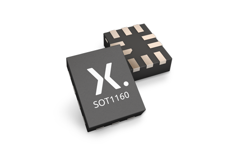
| 74AUP2G97GU | 74AUP2G97GUX (935304484115) |
Active | aV |
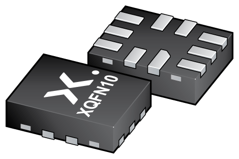
XQFN10 (SOT1160-1) |
SOT1160-1 | SOT1160-1_115 |
下表中的所有产品型号均已停产 。
| 型号 | 可订购的器件编号,(订购码(12NC)) | 状态 | 标示 | 封装 | 外形图 | 回流焊/波峰焊 | 包装 |
|---|---|---|---|---|---|---|---|
| 74AUP2G97GF | 74AUP2G97GFX (935304482115) |
Obsolete | aV |
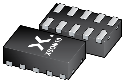
XSON10 (SOT1081-2) |
SOT1081-2 | 暂无信息 |
环境信息
| 型号 | 可订购的器件编号 | 化学成分 | RoHS | RHF指示符 |
|---|---|---|---|---|
| 74AUP2G97DP | 74AUP2G97DPJ | 74AUP2G97DP |
|
|
| 74AUP2G97GU | 74AUP2G97GUX | 74AUP2G97GU |
|
|
下表中的所有产品型号均已停产 。
| 型号 | 可订购的器件编号 | 化学成分 | RoHS | RHF指示符 |
|---|---|---|---|---|
| 74AUP2G97GF | 74AUP2G97GFX | 74AUP2G97GF |
|
|
文档 (15)
| 文件名称 | 标题 | 类型 | 日期 |
|---|---|---|---|
| 74AUP2G97 | Low-power dual PCB configurable multiple function gate | Data sheet | 2023-08-01 |
| AN90063 | Questions about package outline drawings | Application note | 2025-03-12 |
| Nexperia_document_guide_MiniLogic_PicoGate_201901 | PicoGate leaded logic portfolio guide | Brochure | 2019-01-07 |
| Nexperia_document_guide_MiniLogic_MicroPak_201808 | MicroPak leadless logic portfolio guide | Brochure | 2018-09-03 |
| SOT552-1 | 3D model for products with SOT552-1 package | Design support | 2020-01-22 |
| SOT1160-1 | 3D model for products with SOT1160-1 package | Design support | 2019-10-03 |
| Nexperia_document_leaflet_Logic_AUP_technology_portfolio_201904 | Nexperia_document_leaflet_Logic_AUP_technology_portfolio_201904 | Leaflet | 2019-04-12 |
| Nexperia_package_poster | Nexperia package poster | Leaflet | 2020-05-15 |
| TSSOP10_SOT552_mk | plastic, thin shrink small outline package; 10 leads; 0.5 mm pitch; 3 mm x 3 mm x 1.1 mm body | Marcom graphics | 2017-01-28 |
| XQFN10_SOT1160-1_mk | plastic, extremely thin quad flat package; no leads; 10 terminals; 0.4 mm pitch; 1.4 mm x 1.8 mm x 0.5 mm body | Marcom graphics | 2017-01-28 |
| SOT552-1 | plastic, thin shrink small outline package; 10 leads; 0.5 mm pitch; 3 mm x 3 mm x 1.1 mm body | Package information | 2025-03-19 |
| SOT1081-2 | plastic, leadless extremely thin small outline package; 10 terminals; 0.35 mm pitch; 1.7 mm x 1 mm x 0.5 mm body | Package information | 2020-04-21 |
| SOT1160-1 | plastic, leadless extremely thin quad flat package; 10 terminals; 0.4 mm pitch; 1.4 mm x 1.8 mm x 0.5 mm body | Package information | 2022-06-07 |
| Nexperia_Selection_guide_2023 | Nexperia Selection Guide 2023 | Selection guide | 2023-05-10 |
| SSOP-TSSOP-VSO-WAVE | Footprint for wave soldering | Wave soldering | 2009-10-08 |
支持
如果您需要设计/技术支持,请告知我们并填写 应答表 我们会尽快回复您。
Ordering, pricing & availability
样品
作为 Nexperia 的客户,您可以通过我们的销售机构订购样品。
如果您没有 Nexperia 的直接账户,我们的全球和地区分销商网络可为您提供 Nexperia 样品支持。查看官方经销商列表。