
参数类型
| 型号 | VCC (V) | Logic switching levels | Output drive capability (mA) | tpd (ns) | fmax (MHz) | Nr of bits | Power dissipation considerations | Tamb (°C) | Rth(j-a) (K/W) | Ψth(j-top) (K/W) | Rth(j-c) (K/W) | Package name |
|---|---|---|---|---|---|---|---|---|---|---|---|---|
| 74LVC2G08DC-Q100 | 1.65 - 5.5 | CMOS/LVTTL | ± 24 | 2.1 | 150 | 2 | low | -40~125 | 200 | 32.4 | 110 | VSSOP8 |
| 74LVC2G08DP-Q100 | 1.65 - 5.5 | CMOS/LVTTL | ± 24 | 2.1 | 150 | 2 | low | -40~125 | 210 | 18.8 | 104 | TSSOP8 |
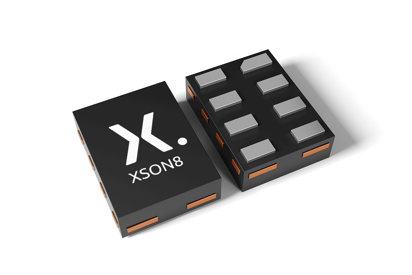
| 74LVC2G08GS-Q100 | 1.65 - 5.5 | CMOS/LVTTL | ± 24 | 2.1 | 150 | 2 | low | -40~125 | 269 | 9.7 | 141 | XSON8 |
封装
| 型号 | 可订购的器件编号,(订购码(12NC)) | 状态 | 标示 | 封装 | 外形图 | 回流焊/波峰焊 | 包装 |
|---|---|---|---|---|---|---|---|
| 74LVC2G08DC-Q100 | 74LVC2G08DC-Q100H (935301554125) |
Active | V08 |
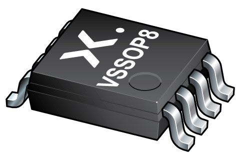
VSSOP8 (SOT765-1) |
SOT765-1 | SOT765-1_125 | |
| 74LVC2G08DP-Q100 | 74LVC2G08DP-Q100H (935301555125) |
Active | V08 |
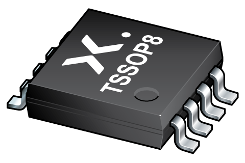
TSSOP8 (SOT505-2) |
SOT505-2 | SOT505-2_125 | |
| 74LVC2G08GS-Q100 | 74LVC2G08GS-Q100X (935690675115) |
Active | VE |
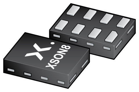
XSON8 (SOT1203) |
SOT1203 |
REFLOW_BG-BD-1
|
SOT1203_115 |
环境信息
| 型号 | 可订购的器件编号 | 化学成分 | RoHS | RHF指示符 |
|---|---|---|---|---|
| 74LVC2G08DC-Q100 | 74LVC2G08DC-Q100H | 74LVC2G08DC-Q100 |
|
|
| 74LVC2G08DP-Q100 | 74LVC2G08DP-Q100H | 74LVC2G08DP-Q100 |
|
|
| 74LVC2G08GS-Q100 | 74LVC2G08GS-Q100X | 74LVC2G08GS-Q100 |
|
|
文档 (21)
| 文件名称 | 标题 | 类型 | 日期 |
|---|---|---|---|
| 74LVC2G08_Q100 | Dual 2-input AND gate | Data sheet | 2023-08-16 |
| AN10161 | PicoGate Logic footprints | Application note | 2002-10-29 |
| AN11009 | Pin FMEA for LVC family | Application note | 2019-01-09 |
| AN90063 | Questions about package outline drawings | Application note | 2025-03-12 |
| 001aah788 | Block diagram: 74AUP2G08DC, 74AUP2G08GD, 74AUP2G08GM, 74AUP2G08GT, 74LVC2G08DC, 74LVC2G08DP, 74LVC2G08GD, 74LVC2G08GM, 74LVC2G08GT | Block diagram | 2009-11-04 |
| Nexperia_document_guide_MiniLogic_PicoGate_201901 | PicoGate leaded logic portfolio guide | Brochure | 2019-01-07 |
| Nexperia_document_guide_MiniLogic_MicroPak_201808 | MicroPak leadless logic portfolio guide | Brochure | 2018-09-03 |
| SOT765-1 | 3D model for products with SOT765-1 package | Design support | 2020-01-22 |
| SOT505-2 | 3D model for products with SOT505-2 package | Design support | 2019-01-18 |
| SOT1203 | 3D model for products with SOT1203 package | Design support | 2023-02-02 |
| lvc2g08 | 74LVC2G08 IBIS model | IBIS model | 2014-10-20 |
| Nexperia_document_leaflet_Logic_X2SON_packages_062018 | X2SON ultra-small 4, 5, 6 & 8-pin leadless packages | Leaflet | 2018-06-05 |
| Nexperia_package_poster | Nexperia package poster | Leaflet | 2020-05-15 |
| VSSOP8_SOT765-1_mk | plastic, very thin shrink small outline package; 8 leads; 0.5 mm pitch; 2 mm x 2.3 mm x 1 mm body | Marcom graphics | 2017-01-28 |
| XSON8_SOT1203_mk | plastic, leadless extremely thin small outline package; 8 terminals; 0.35 mm pitch; 1.35 mm x 1 mm x 0.35 mm body | Marcom graphics | 2019-02-04 |
| SOT765-1 | plastic, very thin shrink small outline package; 8 leads; 0.5 mm pitch; 2 mm x 2.3 mm x 1 mm body | Package information | 2022-06-03 |
| SOT505-2 | plastic, thin shrink small outline package; 8 leads; 0.65 mm pitch; 3 mm x 3 mm x 1.1 mm body | Package information | 2022-06-03 |
| SOT1203 | plastic, leadless extremely thin small outline package; 8 terminals; 0.35 mm pitch; 1.35 mm x 1 mm x 0.35 mm body | Package information | 2022-06-03 |
| REFLOW_BG-BD-1 | Reflow soldering profile | Reflow soldering | 2021-04-06 |
| Nexperia_Selection_guide_2023 | Nexperia Selection Guide 2023 | Selection guide | 2023-05-10 |
| MAR_SOT1203 | MAR_SOT1203 Topmark | Top marking | 2013-06-03 |
支持
如果您需要设计/技术支持,请告知我们并填写 应答表 我们会尽快回复您。
模型
Ordering, pricing & availability
样品
作为 Nexperia 的客户,您可以通过我们的销售机构订购样品。
如果您没有 Nexperia 的直接账户,我们的全球和地区分销商网络可为您提供 Nexperia 样品支持。查看官方经销商列表。