可订购部件
| 型号 | 可订购的器件编号 | 订购代码(12NC) | 封装 | 从经销商处购买 |
|---|---|---|---|---|
| 74AUP1T97GW-Q100 | 74AUP1T97GW-Q100H | 935691179125 | SOT363-2 | 订单产品 |
Register once, drag and drop ECAD models into your CAD tool and speed up your design.
Click here for more informationLow-power configurable gate with voltage-level translator
The 74AUP1T97-Q100 is a configurable multiple function gate with level translating, Schmitt-trigger inputs. The device can be configured as any of the following logic functions MUX, AND, OR, NAND, NOR, inverter and buffer; using the 3-bit input. All inputs can be connected directly to VCC or GND. Low threshold Schmitt trigger inputs allow these devices to be driven by 1.8 V logic levels in 3.3 V applications. This device ensures very low static and dynamic power consumption across the entire VCC range from 2.3 V to 3.6 V. This device is fully specified for partial power down applications using IOFF. The IOFF circuitry disables the output, preventing the potentially damaging backflow current through the device when it is powered down.
This product has been qualified to the Automotive Electronics Council (AEC) standard Q100 (Grade 1) and is suitable for use in automotive applications.
Automotive product qualification in accordance with AEC-Q100 (Grade 1)
Specified from -40 °C to +85 °C and from -40 °C to +125 °C
Wide supply voltage range from 2.3 V to 3.6 V
CMOS low power dissipation
High noise immunity
Overvoltage tolerant inputs to 3.6 V
Low noise overshoot and undershoot < 10 % of VCC
IOFF circuitry provides partial power-down mode operation
Latch-up performance exceeds 100 mA per JESD 78 Class II
Low static power consumption; ICC = 1.5 μA (maximum)
Complies with JEDEC standards:
JESD8-12 (0.8 V to 1.3 V)
JESD8-11 (0.9 V to 1.65 V)
JESD8-7 (1.65 V to 1.95 V)
JESD8-5 (2.3 V to 2.7 V)
JESD8C (2.7 V to 3.6 V)
ESD protection:
HBM: ANSI/ESDA/JEDEC JS-001 class 3A exceeds 5000 V
CDM: ANSI/ESDA/JEDEC JS-002 class C3 exceeds 1000 V
| 型号 | VCC (V) | Logic switching levels | Output drive capability (mA) | tpd (ns) | fmax (MHz) | Nr of bits | Power dissipation considerations | Tamb (°C) | Rth(j-a) (K/W) | Ψth(j-top) (K/W) | Rth(j-c) (K/W) | Package name |
|---|---|---|---|---|---|---|---|---|---|---|---|---|
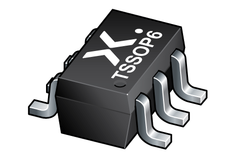
| 74AUP1T97GW-Q100 | 2.3 - 3.6 | CMOS | ± 4 | 3.9 | 70 | 1 | ultra low | -40~125 | 264 | 38.6 | 153 | TSSOP6 |
| 型号 | 可订购的器件编号,(订购码(12NC)) | 状态 | 标示 | 封装 | 外形图 | 回流焊/波峰焊 | 包装 |
|---|---|---|---|---|---|---|---|
| 74AUP1T97GW-Q100 | 74AUP1T97GW-Q100H (935691179125) |
Active | 59 |
TSSOP6 (SOT363-2) |
SOT363-2 | SOT363-2_125 |
| 文件名称 | 标题 | 类型 | 日期 |
|---|---|---|---|
| 74AUP1T97_Q100 | Low-power configurable gate with voltage-level translator | Data sheet | 2023-07-17 |
| AN90063 | Questions about package outline drawings | Application note | 2025-06-13 |
| SOT363-2 | 3D model for products with SOT363-2 package | Design support | 2023-02-02 |
| SOT363-2 | plastic thin shrink small outline package; 6 leads; body width 1.25 mm | Package information | 2022-11-21 |
| SOT363-2_125 | TSSOP6 ; Reel pack for SMD, 7"; Q3/T4 product orientation | Packing information | 2022-11-04 |
| 74AUP1T97GW-Q100_Nexperia_Product_Reliability | 74AUP1T97GW-Q100 Nexperia Product Reliability | Quality document | 2025-03-20 |
The Nexperia Longevity Program is aimed to provide our customers information from time to time about the expected time that our products can be ordered. The NLP is reviewed and updated regularly by our Executive Management Team. View our longevity program here.
| 文件名称 | 标题 | 类型 | 日期 |
|---|---|---|---|
| SOT363-2 | 3D model for products with SOT363-2 package | Design support | 2023-02-02 |
| 型号 | Orderable part number | Ordering code (12NC) | 状态 | 包装 | Packing Quantity | 在线购买 |
|---|---|---|---|---|---|---|
| 74AUP1T97GW-Q100 | 74AUP1T97GW-Q100H | 935691179125 | Active | SOT363-2_125 | 3,000 |
|
作为 Nexperia 的客户,您可以通过我们的销售机构订购样品。
如果您没有 Nexperia 的直接账户,我们的全球和地区分销商网络可为您提供 Nexperia 样品支持。查看官方经销商列表。
The interactive datasheets are based on the Nexperia MOSFET precision electrothermal models. With our interactive datasheets you can simply specify your own conditions interactively. Start by changing the values of the conditions. You can do this by using the sliders in the condition fields. By dragging the sliders you will see how the MOSFET will perform at the new conditions set.