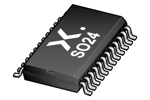
Register once, drag and drop ECAD models into your CAD tool and speed up your design.
Click here for more information74LVC4245AD
Octal dual supply translating transceiver; 3-state
The 74LVC4245A is an octal dual supply translating transceiver featuring 3-state bus compatible outputs in both send and receive directions. It is designed to interface between a 3 V and 5 V bus in a mixed 3 V and 5 V supply environment. The device features an output enable input (OE) and a send/receive input (DIR) for direction control. A HIGH on OE causes the outputs to assume a high-impedance OFF-state, effectively isolating the buses. In suspend mode, when either supply is zero, there is no current path between supplies. VCCA ≥ VCCB, except in suspend mode. Schmitt-trigger action at all inputs makes the circuit tolerant of slower input rise and fall times.
Alternatives
Features and benefits
5 V tolerant inputs/outputs, for interfacing with 5 V logic
Wide supply voltage range:
3 V bus (VCC(B)): 1.5 V to 3.6 V
5 V bus (VCC(A)): 1.5 V to 5.5 V
CMOS low-power consumption
TTL interface capability at 3.3 V
Overvoltage tolerant control inputs to 5.5 V
High-impedance when VCC(A) = 0 V
Complies with JEDEC standard no. JESD8B/JESD36
Latch-up performance meets requirements of JESD78 Class 1
ESD protection:
HBM: ANSI/ESDA/JEDEC JS-001 class 2 exceeds 2000 V
CDM: ANSI/ESDA/JEDEC JS-002 class C3 exceeds 1000 V
Multiple package options
Specified from -40 °C to +85 °C and -40 °C to +125 °C
PCB Symbol, Footprint and 3D Model
| Model Name | 描述 |
|---|---|
|
|
封装
下表中的所有产品型号均已停产 。
| 型号 | 可订购的器件编号,(订购码(12NC)) | 状态 | 标示 | 封装 | 外形图 | 回流焊/波峰焊 | 包装 |
|---|---|---|---|---|---|---|---|
| 74LVC4245AD | 74LVC4245AD,118 (935260749118) |
Withdrawn / End-of-life |

SO24 (SOT137-1) |
SOT137-1 |
SO-SOJ-WAVE
WAVE_BG-BD-1 |
SOT137-1_118 | |
| 74LVC4245AD,112 (935260749112) |
Obsolete | 暂无信息 |
环境信息
下表中的所有产品型号均已停产 。
| 型号 | 可订购的器件编号 | 化学成分 | RoHS | RHF指示符 |
|---|---|---|---|---|
| 74LVC4245AD | 74LVC4245AD,118 | 74LVC4245AD |
|
|
| 74LVC4245AD | 74LVC4245AD,112 | 74LVC4245AD |
|
|
Series
文档 (13)
| 文件名称 | 标题 | 类型 | 日期 |
|---|---|---|---|
| 74LVC4245A | Octal dual supply translating transceiver; 3-state | Data sheet | 2024-11-29 |
| AN11009 | Pin FMEA for LVC family | Application note | 2019-01-09 |
| AN263 | Power considerations when using CMOS and BiCMOS logic devices | Application note | 2023-02-07 |
| AN90063 | Questions about package outline drawings | Application note | 2025-06-13 |
| Nexperia_document_guide_Logic_translators | Nexperia Logic Translators | Brochure | 2021-04-12 |
| SOT137-1 | 3D model for products with SOT137-1 package | Design support | 2020-01-22 |
| lvc4245a | lvc4245a IBIS model | IBIS model | 2013-04-09 |
| Nexperia_package_poster | Nexperia package poster | Leaflet | 2020-05-15 |
| SOT137-1 | plastic, small outline package; 24 leads; 1.27 mm pitch; 15.4 mm x 7.5 mm x 2.65 mm body | Package information | 2022-06-21 |
| 74LVC4245AD_Nexperia_Product_Reliability | 74LVC4245AD Nexperia Product Reliability | Quality document | 2022-05-04 |
| lvc | lvc Spice model | SPICE model | 2013-05-07 |
| SO-SOJ-WAVE | Footprint for wave soldering | Wave soldering | 2009-10-08 |
| WAVE_BG-BD-1 | Wave soldering profile | Wave soldering | 2021-09-08 |
Longevity
The Nexperia Longevity Program is aimed to provide our customers information from time to time about the expected time that our products can be ordered. The NLP is reviewed and updated regularly by our Executive Management Team. View our longevity program here.
PCB Symbol, Footprint and 3D Model
| Model Name | 描述 |
|---|---|
|
|
How does it work?
The interactive datasheets are based on the Nexperia MOSFET precision electrothermal models. With our interactive datasheets you can simply specify your own conditions interactively. Start by changing the values of the conditions. You can do this by using the sliders in the condition fields. By dragging the sliders you will see how the MOSFET will perform at the new conditions set.