
特性
-
Wide supply voltage range:
-
VCCI: 0.9 V to 5.5 V
-
VCCO: 0.9 V to 5.5 V
-
-
Low input capacitance; CI = 1.5 pF (typical)
-
Low output capacitance; CO = 3.8 pF (typical)
-
Low dynamic power consumption; CPD = 0.4 pF at VCCI = 1.2 V (typical)
-
Low dynamic power consumption; CPD = 11 pF at VCCO = 5 V (typical)
-
Low static power consumption; ICCI = 0.1 µA (25 °C maximum)
-
Low static power consumption; ICCO = 1.0 µA (25 °C maximum)
-
High noise immunity
-
Complies with JEDEC standard:
-
JESD8-12 (1.1 V to 1.3 V; A input)
-
JESD8-11 (1.4 V to 1.6 V)
-
JESD8-7 (1.65 V to 1.95 V)
-
JESD8-5 (2.3 V to 2.7 V)
-
JESD8C (2.7 V to 3.6 V)
-
JESD12-6 (4.5 V to 5.5 V)
-
-
ESD protection:
-
HBM: ANSI/ESDA/JEDEC JS-001 class 2 exceeds 2000 V
-
CDM: ANSI/ESDA/JEDEC JS-002 class C3 exceeds 1000 V
-
-
Latch-up performance exceeds 100 mA per JESD78D Class II
-
Inputs accept voltages up to 5.5 V
-
Low noise overshoot and undershoot < 10% of VCCO
-
IOFF circuitry provides partial power-down mode operation
-
Multiple package options
-
Specified from −40 °C to +125 °C
封装
| 型号 | 封装 | 尺寸版本 | 回流焊/波峰焊 | 包装 | 状态 | 标示 | 可订购的器件编号,(订购码(12NC)) |
|---|---|---|---|---|---|---|---|
| AXP1T34GM | 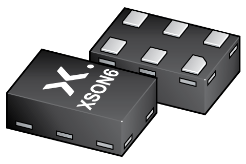 XSON6 (SOT886) | SOT886 | REFLOW_BG-BD-1 | SOT886_115 | Active | r3 | AXP1T34GMX ( 9356 916 27115 ) |
| AXP1T34GS |  XSON6 (SOT1202) | SOT1202 | REFLOW_BG-BD-1 | SOT1202_125 | Active | r3 | AXP1T34GSH ( 9356 916 26125 ) |
| AXP1T34GW | 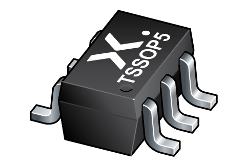 TSSOP5 (SOT353-1) | SOT353-1 | WAVE_BG-BD-1 | SOT353-1_125 | Active | r3 | AXP1T34GWH ( 9356 916 24125 ) |
| AXP1T34GX | 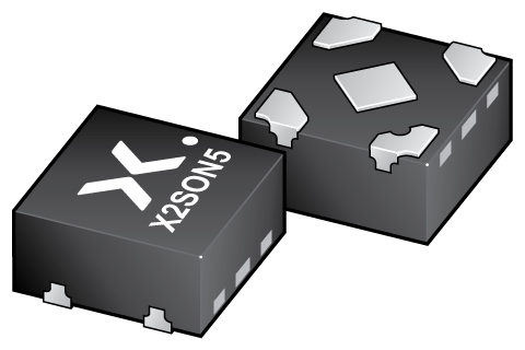 X2SON5 (SOT1226-3) | SOT1226-3 | SOT1226-3_125 | Active | r3 | AXP1T34GXH ( 9356 915 73125 ) |
环境信息
| 型号 | 可订购的器件编号 | 化学成分 | RoHS | RHF指示符 | 无铅转换日期 |
|---|---|---|---|---|---|
| AXP1T34GM | AXP1T34GMX | AXP1T34GM | |||
| AXP1T34GS | AXP1T34GSH | AXP1T34GS | |||
| AXP1T34GW | AXP1T34GWH | AXP1T34GW | |||
| AXP1T34GX | AXP1T34GXH | AXP1T34GX |
文档 (10)
| 文件名称 | 标题 | 类型 | 日期 |
|---|---|---|---|
| AXP1T34 | Dual supply translating buffer | Data sheet | 2023-12-01 |
| REFLOW_BG-BD-1 | Reflow soldering profile | Reflow soldering | 2021-04-06 |
| MAR_SOT1202 | MAR_SOT1202 Topmark | Top marking | 2013-06-03 |
| SOT1202 | plastic, leadless extremely thin small outline package; 6 terminals; 0.35 mm pitch; 1 mm x 1mm x 0.35 mm body | Package information | 2022-06-01 |
| WAVE_BG-BD-1 | Wave soldering profile | Wave soldering | 2021-09-08 |
| SOT353-1 | plastic thin shrink small outline package; 5 leads; body width 1.25 mm | Package information | 2022-11-15 |
| MAR_SOT886 | MAR_SOT886 Topmark | Top marking | 2013-06-03 |
| SOT886 | plastic, leadless extremely thin small outline package; 6 terminals; 0.5 mm pitch; 1 mm x 1.45 mm x 0.5 mm body | Package information | 2022-06-01 |
| REFLOW_BG-BD-1 | Reflow soldering profile | Reflow soldering | 2021-04-06 |
| SOT1226-3 | plastic thermal enhanced extremely thin small outline package; no leads;5 terminals; body 0.8 x 0.8 x 0.32 mm | Package information | 2020-08-27 |
支持
如果您需要设计/技术支持,请告知我们并填写 应答表, 我们会尽快回复您。
样品
安世半导体客户可通过我们的销售机构或直接通过在线样品商店订购样品: https://extranet.nexperia.com.
样品订单通常需要2-4天寄送时间。
如果您尚未取得安世半导体的直接采购帐号,我们的全球与区域经销网络可以协助您取得样品。