双极性晶体管

二极管

ESD保护、TVS、滤波和信号调节ESD保护

MOSFET

SiC power devices

氮化镓场效应晶体管(GaN FET)

绝缘栅双极晶体管(IGBTs)

模拟和逻辑IC

汽车应用认证产品(AEC-Q100/Q101)

80 - 200 V low-power GaN devices

High efficiency in the smallest footprint

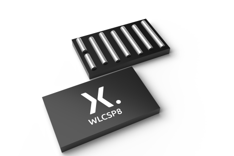
Nexperia’s low-power 80–200 V GaN platform brings the benefits of wide-bandgap technology to compact systems where efficiency, size and system cost are critical. Combining ultra-low RDS(on), low QG and QOSS, and clean, fast switching in compact CSP packages, these devices enable higher switching frequencies, reduced magnetics and increased power density. Ideal for power supplies, audio amplifiers, LiDAR and low-power motor drives, they deliver lower losses, simpler thermal management and significant size reduction. Delivering the efficiency, compactness and integration flexibility increasingly required by today's electronic systems.

产品

型号 描述 状态 快速访问
GAN3R2-100CBE 100 V, 3.2 mOhm Gallium Nitride (GaN) FET in a 3.5 mm x 2.13 mm Wafer Level Chip-Scale Package (WLCSP) Production
GAN7R0-150LBE 150 V, 7 mOhm Gallium Nitride (GaN) FET in a 2.2 mm x 3.2 mm x 0.774 mm Land Grid Array (LGA) package Production
GANE011-080CBA AEC-Q101 qualified 80 V, 11 mOhm Gallium Nitride (GaN) FET in a 1.5 mm x 1.5 mm Wafer Level Chip-Scale Package (WLCSP) Production
GANE2R7-100CBA 100 V, 2.7 mOhm Gallium Nitride (GaN) FET in a 4.45 mm x 2.30 mm Wafer Level Chip-Scale Package (WLCSP) Production
GANE7R0-100CBA 100 V, 7.0 mOhm Gallium Nitride (GaN) FET in a 2.5 mm x 1.5 mm Wafer Level Chip-Scale Package (WLCSP) Production

如果您有支持方面的疑问,请告知我们。如需获得设计支持,请告知我们并填写技术支持表格,我们会尽快回复您。

请访问我们的社区论坛联系我们


交叉参考